SEM Analysis Solutions

Scanning Electron Microscopy (SEM) is a powerful analytical technique used to examine materials at high magnification and resolution. SEM provides detailed imaging of surface features, microstructures, defects and material characteristics that cannot be observed using conventional optical microscopy.

  • 5000+ Projects Delivered

How SEAM Can Help

SEM analysis enables organisations to investigate material performance, identify defects, support failure investigations and better understand product quality. By providing detailed visual and compositional information, SEM helps clients make informed decisions during product development, quality assurance and research projects.

Whether you are examining fracture surfaces, contamination, coatings, surface defects or material structures, SEAM can provide the expertise and analytical capabilities required to support your project.

Key Benefits

  • High-resolution imaging and analysis
  • Failure investigation and root cause analysis
  • Material and surface characterisation
  • Defect and contamination identification
  • Support for product development and validation
Analysis

Failure Analysis

Investigate cracks, fractures, wear mechanisms and material defects.

Analysis

Product Validation

Analysis

Contamination Analysis

Identify foreign materials, particles and manufacturing contamination.

Analysis

R&D Support

Support material development, product innovation and process optimisation.
Equipment & Capabilities

SEAM's advanced SEM systems provide detailed imaging and material analysis capabilities. Combined with complementary techniques such as EDS analysis, FTIR, Raman spectroscopy and XRD, SEM can deliver comprehensive insights into material structure, composition and performance.


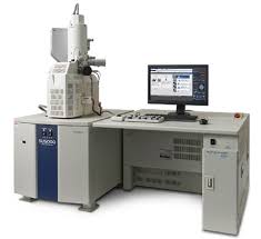
Hitachi SU5000 Scanning Electron Microscope (SEM)

The Hitachi SU5000 Scanning Electron Microscope (SEM) offers high-resolution imaging and versatile analytical capabilities for material characterization. Key features include advanced variable-pressure technology, a wide magnification range, and intuitive operation. It excels in imaging surface morphology and microstructures, as well as elemental analysis through integrated energy-dispersive X-ray spectroscopy (EDS).

  • Advanced equipment
  • Fast technical support
  • Independent expertise
  • Clear reporting
Testimonials

How it Works

  • 1. Submit Enquiry
  • 2. Technical Review
  • 3. Testing / Simulation
  • 4. Report Delivered

Have a project you’d like to discuss?

Submit an Enquiry

Speak directly with SEAM’s experienced industry specialists to discuss your project. Every enquiry is reviewed by highly qualified engineers and technical experts who will recommend the most appropriate testing or analysis approach based on your requirements.

Whether you need independent validation, product development support, quality assurance or failure investigation, we’re here to help. Following completion of the work, you’ll receive a comprehensive technical report outlining the methodology, findings and recommendations, giving you the confidence to make informed engineering and business decisions.

Complete the enquiry form today and a member of our team will be in touch to discuss your requirements and the next steps.

    Case Studies

    Lorem Ipsum is simply dummy text of the printing and typesetting industry. Lorem Ipsum has been the industry's standard dummy text ever since the 1500s, when an unknown

    Projects
    2000 +
    Capabilities
    0 +

    Trusted by Industry

    Frequently Asked Questions

    Learn how SEM analysis provides detailed imaging and material insights to support failure investigations, product development and advanced materials research.

    What is SEM analysis?

    SEM (Scanning Electron Microscopy) uses a focused electron beam to generate high-resolution images of material surfaces and structures.

    SEM is widely used in medical devices, pharmaceuticals, engineering, electronics, polymers and advanced manufacturing.

    Yes. SEM is frequently used to investigate fractures, cracking, wear, corrosion and manufacturing defects.

    Metals, polymers, ceramics, composites, coatings, powders and many other engineering materials can be examined using SEM.

    SEAM combines advanced microscopy capabilities with experienced researchers and complementary analytical techniques to provide comprehensive material investigations.

    Our Equipment

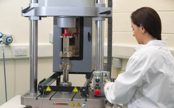
    Instron Electroplus3000

    The ElectroPuls™ E3000 Linear-Torsion is a state-of-the-art, all-electric test instrument engineered for precise dynamic and static tes...